Stiggy
STEM Learning Toy for Middle Schools
Project Scope: Stiggy is a toy RC (radio controlled) car, which through a server on the back-end, will display graphs containing information about the speed and movement of the car. The project comes from a Northeastern University professor who originally designed the car to be sold at Toys"R"Us, but because of various issues, had his contract with the company canceled. With the help of my team, we redesigned the car for him, so that he can continue to pitch it to other companies.
Personal Objective: To design the PCB (printed circuit board) for the power, control, and other components within the car.
Skills learned: I2C Communication, Component Selection, Schematic Design, Component Placement, Routing, Pouring, and Soldering. Upverter was the CAD software that I used.
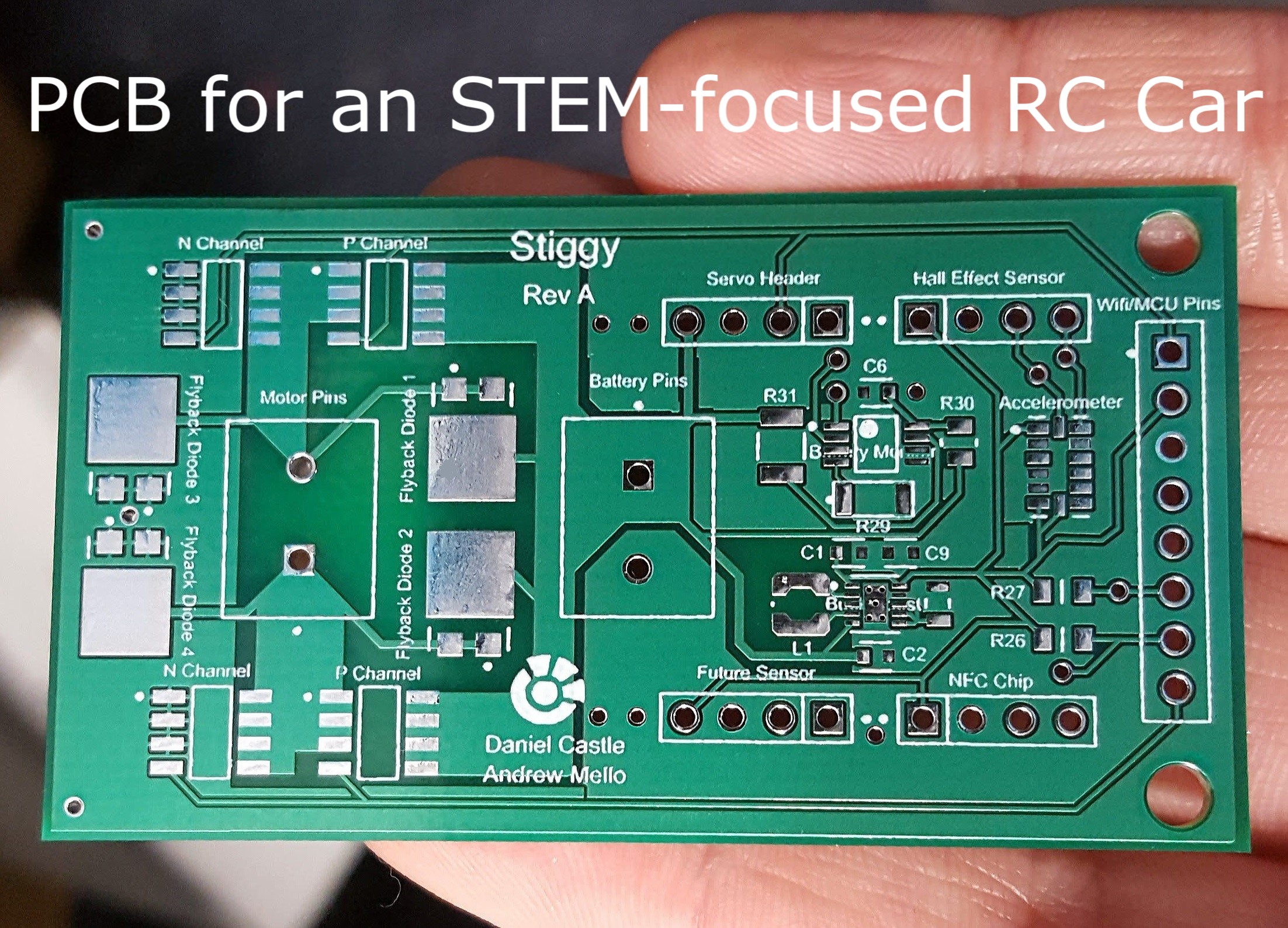
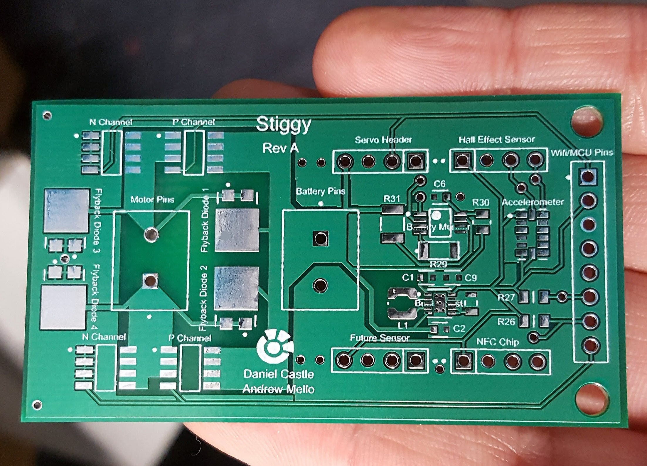
In the image above, the PCB of this project's prototype is shown. The populated version and explanations of the circuit are given below.
Check out this PDF for more information about the project by clicking here.
For a complete Bill of Materials (BOM) incorporated into the PCB, please click here.
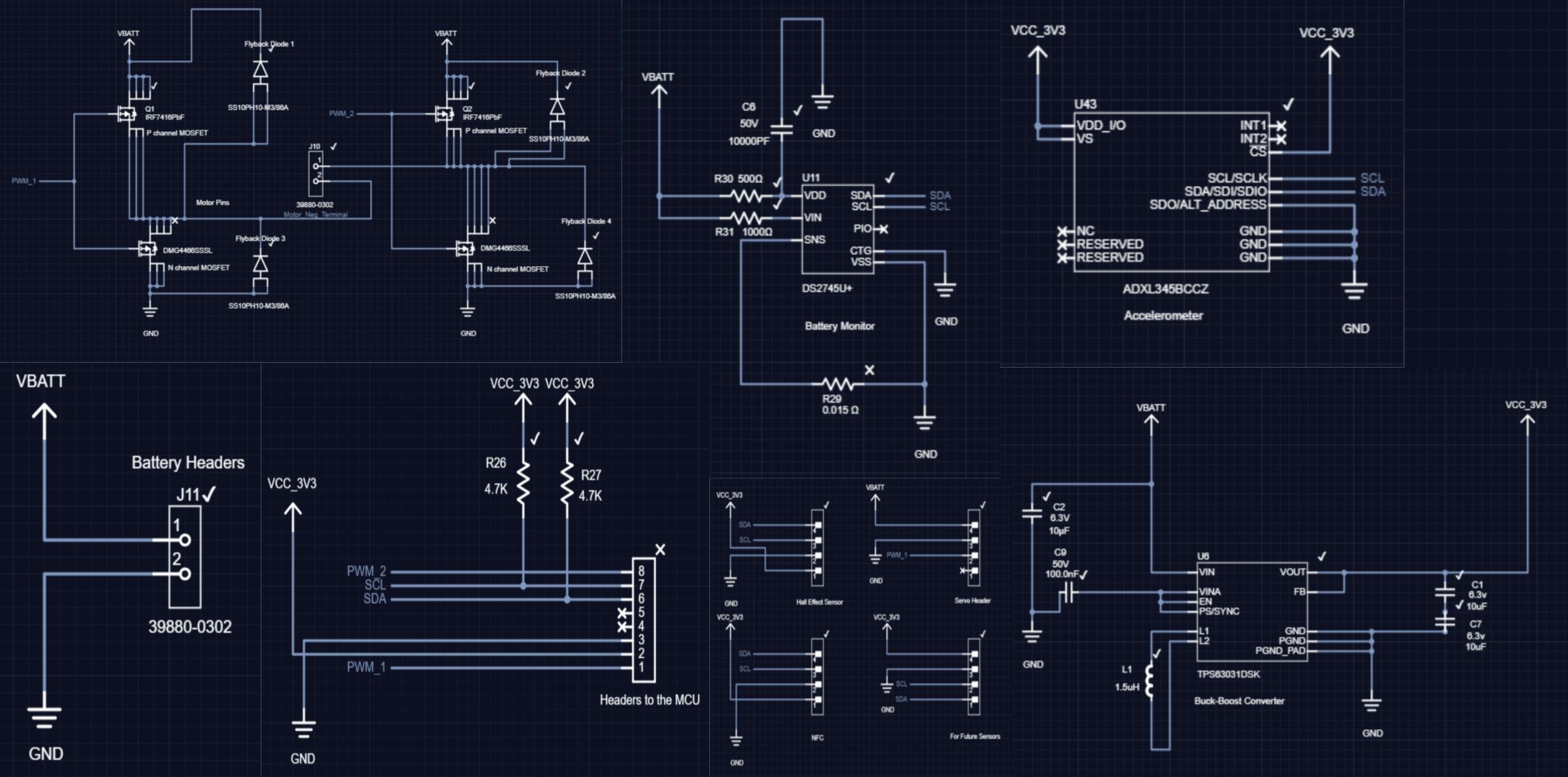 The image to the right is the schematic design of my PCB.
Each major section of the PCB comprised of a dominant feature that formed the basis of that part of the circuit, complete with any capacitors, inductors, or resistors that the dominant component(s) that enabled the feature would need.
The dominant features were: the motor-driving circuit, the battery monitor circuit, the accelerometer circuit, the battery headers for power, the external headers for the external sensors, and the buck-boost converter circuit for stepping up and stepping down the voltage of the battery.
Within the schematic, each section occupied its own space, allowing for easy reference in case any modifications were necessary. Using flags and appropriately-named lines, each element could be wired together virtually, without the need to clutter the board with excessive, redundant, and explicitly-defined lines that criss-crossed the entire schematic.
Once the components were selected and connected via nets, their footprints were then generated and manipulated to achieve the right position, spacing, and orientation on the board.
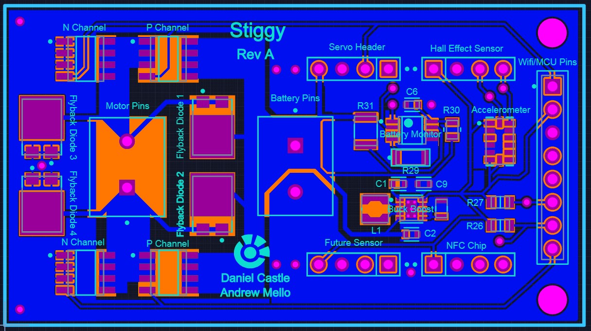 The image to the right shows the design of the top layer of my PCB.
In my 2-layer board, the top layer was primarily focused on providing power (both from the battery and from the buck-boost converter) to the board components. The battery (3.7V) drives the motor, though because the rest of the components required a constant 3.3V to operate, a buck-boost converter was used to regulate the voltage over the entire discharge curve of the battery.
In addition to the 3.7V and 3.3V power traces, two pulse-width modulation (PWM) lines were each routed to two MOSFETS, one line for the n-channel MOSFETS and the other for the p-channel MOSFETS. Through the use of an H-bridge, these lines were used by the MCU on the Wifi chip to control the direction of the motor by applying the voltage from the battery across the motor in the opposite direction (i.e. making the positive terminal now, in effect, negative and vice versa) without having to switch the leads.
To reduce any errant electromagnetic effects that the motor and power circuits would have on the rest of the components if they were too close to those components, both circuits were placed as far left on the PCB as possible, with the rest of the components on the right. In this way, the large current (around 8 Amps) drawn from the battery and the inductive spikes from driving the motor in different directions (as well as the battery's normally larger voltage level, as determined by its discharge curve) would least likely impact the performance of the rest of the components.
To mitigate sudden voltage spikes seen across an inductive load when its supply current is suddenly reduced or interrupted
(AKA, whenever the motor changes direction from forward to reverse, or vise versa), flyback diodes were incorporated into my design.
These flyback diodes return the inductive spikes to the supply instead of moving through the MOSFETs, which could destroy the transistors if not handled accordingly.
Specifically, Schottky diodes were used, as they have a low forward voltage and an extremely small reverse recovery time, giving a fast switching time at a smaller voltage level.
To attach to the car, the two larger holes on the far right are drilled for the stabilization of the PCB within its housing, enabled through two rods that fit snugly within those holes.
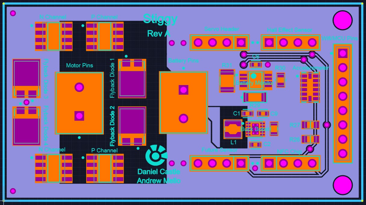 The image to the right shows the design of the bottom layer of my PCB.
In my 2-layer board, the bottom layer was primarily focused on providing the I2C data and clock lines to the board components that required them.
I2C is a serial communication bus where multiple devices, called "slaves", can be connected to one or more "master" devices. The beauty of I2C is that only those two lines are necessary, regardless of how many devices are on the network. As Stiggy is only in its first revision, more components will definitely be added at a later date, and updating the PCB without extensive reworking of traces was seen as paramount.
Every external sensor (servo, hall effect sensor, NFC chip, and one future sensor) and every internal sensor (battery monitor and accelerometer) needed to be connected using I2C. With the Wifi chip, and its attached MCU, as the brains of the car, the devices could both send and receive data as the car needed.
These sensors allowed us to:
1. turn the car (servo)
2. measure wheel speed (hall effect sensor)
3. connect to nearby cars (NFC chip)
4. allow for further development down the line (future sensor)
5. measure battery life (battery monitor)
6. track the forces on the car (accelerometer).
*Note: PWM was not handled using I2C due to its potential to hog the data line, especially if more devices are implemented.
The rest of the bottom layer was used as a ground plane, which served to buffer the sensitive I2C lines from the high voltages and current drawn from the battery.
Vias also connected both layers together on their respective ground planes, ensuring one universal reference point for ground along the entire circuit.
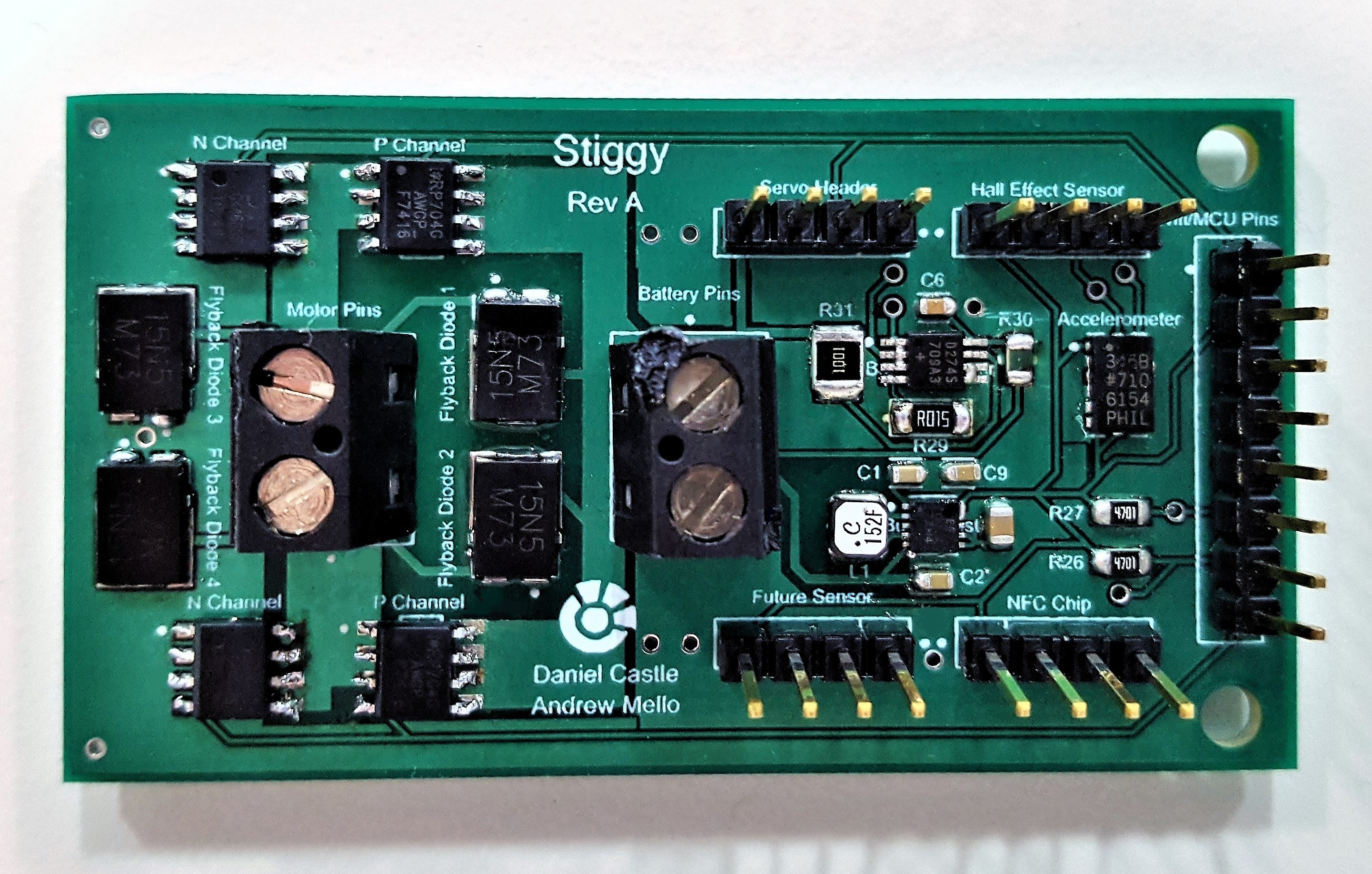
 The image to the right shows the top layer of my PCB, straight from the manufacturer.
With the dimensions of 53mm x 35mm, the board easily fits into my hand.
The silkscreen shows which components go on the board, and where they need to be soldered. Makes life a little easier than scrutinizing schematics and comparing part numbers, so it was definitely well worth it.
On the board, most of the components used pads, with little room for traditional solder. Therefore, I broke out my new favorite toy: solder paste.
 The image to the right shows the populated top layer of the PCB.
With the small-scale nature of the footprints, the lovely, all-you-need-is-a-little-hot-air solder paste was used to join most of the components to the board.
Lesson for next time: expand the footprints, because right now they are a *perfect* fit, but they need to be larger if I'll have any chance to solder them without soldering paste.
But hey, just because something's hard doesn't mean I'm not gonna try it! Therefore, I tried my hand at soldering the MOSFETs with the soldering iron. And yes, it was just as difficult as I thought it would be.
I also soldered the headers and pins with the soldering iron, as they are both through-hole, not surface mount.
Pro tip: don't touch plastic to a hot soldering iron. See those battery pins? Now see that burnt plastic? Yep. Don't do it.
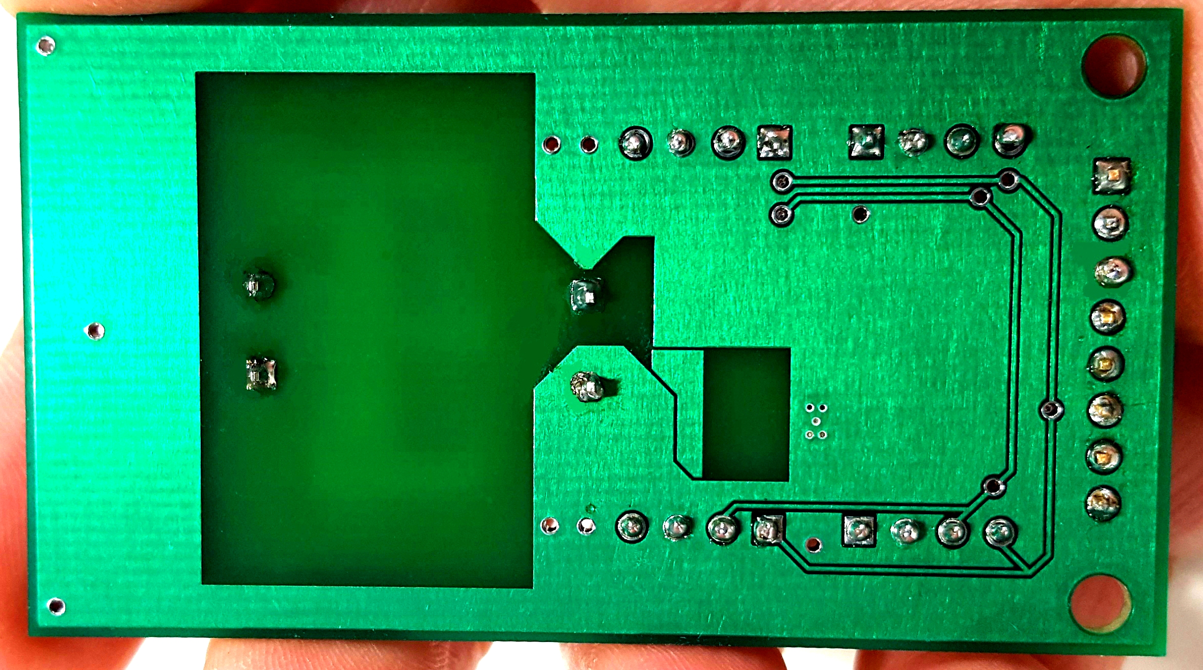 The image to the right shows the bottom layer of my PCB, with the components soldered on.
To minimize the effects that voltage and current spikes would have across the motor circuit, the big area in the center was left intentionally disconnected from the rest of the circuit, as even the ground planes would be subject to them.
That lighter region in the dark area is exactly that concept: the outlines of the two flyback diodes that are connected to both the motor and the battery, which function as the primary outlet for the inductive voltage spike from the motor. Magnetic fields in ground planes can be a recipe for disaster that purposeful avoidance of nearby copper can help prevent.
As the inductor (necessary for the buck-boost converter) would similarly effect the rest of the circuit, it was also separated from the circuit.